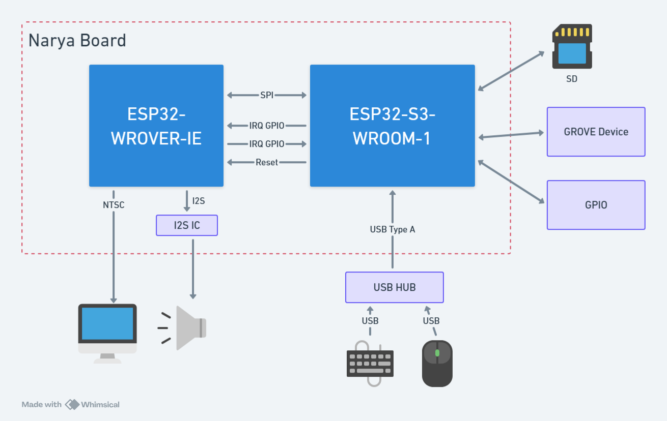
Hardware
Specifications for the connectors and pin assignments of the narya-board.
Note
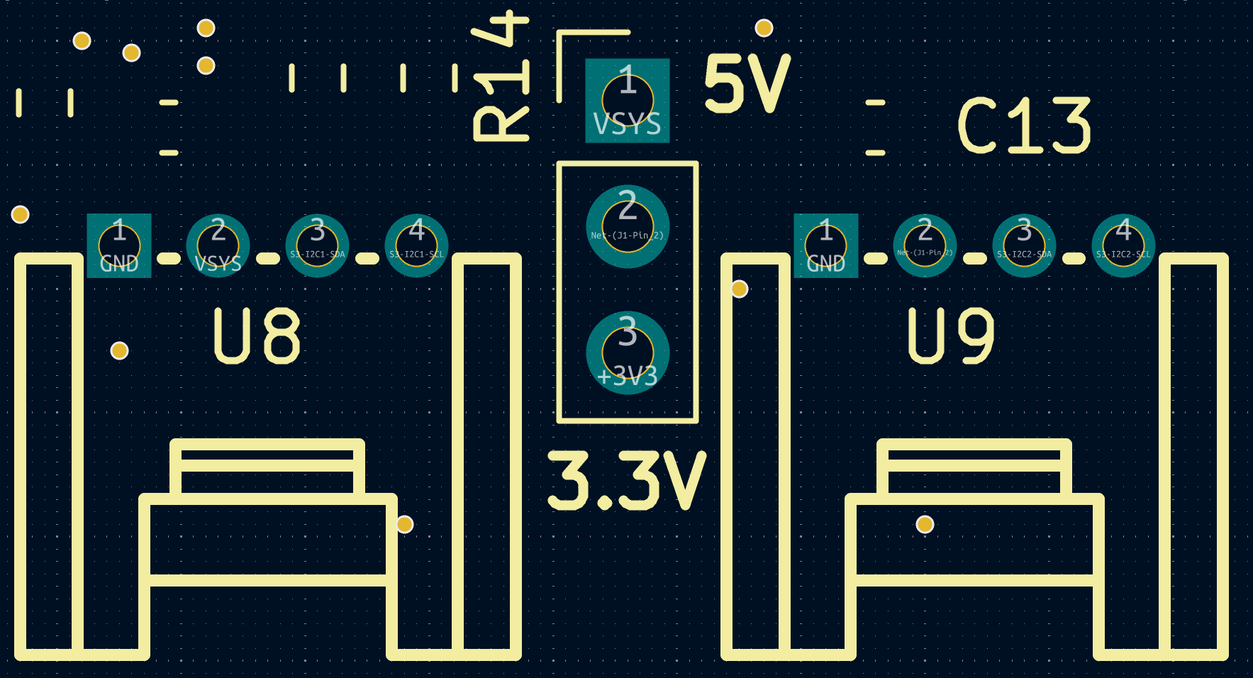
For schematics, KiCAD design files, and board photos, see the narya-board repository.
Overview
| Item | Details |
|---|---|
| Main MCU (fmrb-core) | ESP32-S3-WROOM-1-N16R8 (16MB Flash + 8MB PSRAM) |
| Sub MCU (fmrb-graphics-audio) | ESP32-WROVER-E/IE (with PSRAM) |
| Inter-MCU Communication | UART1 (921600 bps, CTS/RTS flow control) |
| Video Output | NTSC composite (using LovyanGFX CVBS) |
| Audio Output | I2S DAC (NES APU emulator) |
| Storage | Internal LittleFS (16MB) + SD card (FAT32, SPI connection) |
Power Supply
| Item | Value |
|---|---|
| Input | USB Type-C (5V) |
| Internal Regulator | 3.3V |
| Recommended Power | Stable USB supply of 1A or more |
Video Output
| Item | Value |
|---|---|
| Connector | RCA (pin jack, yellow) |
| Signal Format | NTSC composite |
| Standard Resolution | 320 x 240 |
| Color | RGB332 (256 colors) |
If colors appear different due to variations in CRT monitors or capture devices, you can adjust them using FmrbGfx#set_output_level / set_chroma_level.
Audio Output
| Item | Value |
|---|---|
| Connector | 3.5mm stereo mini jack |
| Signal | I2S to DAC analog output |
| Output Level | Line-level equivalent |
The NES APU emulator runs with 4 channels: 2 square waves + 1 triangle wave + 1 noise channel. See FmrbAudio and Audio File Formats for details.
GROVE
The board has 2 GROVE connectors. Listed from left: GND, Power, Sig1, Sig2. The connections are as follows:
| Connector | Sig1 | Sig2 | Notes |
|---|---|---|---|
| GROVE 1 | GPIO 14/I2C1-SDA | GPIO 21/I2C1-SCL | For I2C / shared with RTC (RX8900, address: 0x32). 10K pull-up resistors present |
| GROVE 2 | GPIO 47 | GPIO 48 | General purpose. No pull-up resistors. Power source selectable |
GROVE 1 shares the I2C bus with the RTC, so be careful about address conflicts.
GROVE 2 has no pull-up resistors on the signal lines, and the power supply method can be changed via pin headers, so it can be used freely for GPIO, UART, RMT, and other purposes.
Pin Assignments
ESP32-S3 Pin Assignment
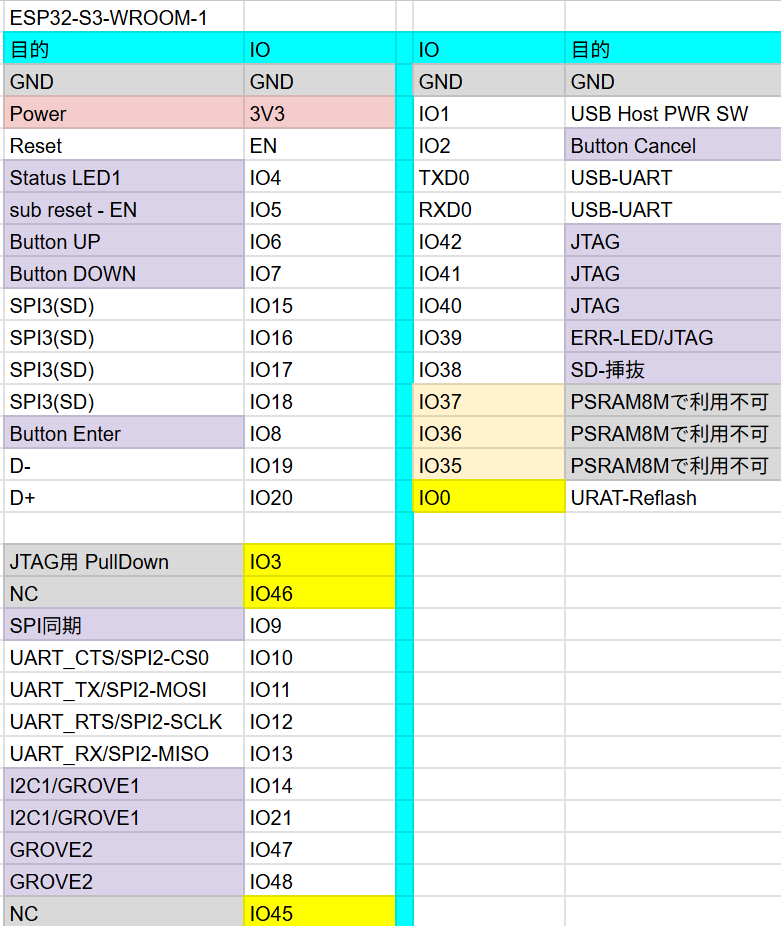
GPIO40 is connected to the INT pin of the RX8900 with a pull-up resistor.
JTAG functionality has not been verified. If you want to use it, you need to remove the 0-ohm resistor. See the schematics for details.
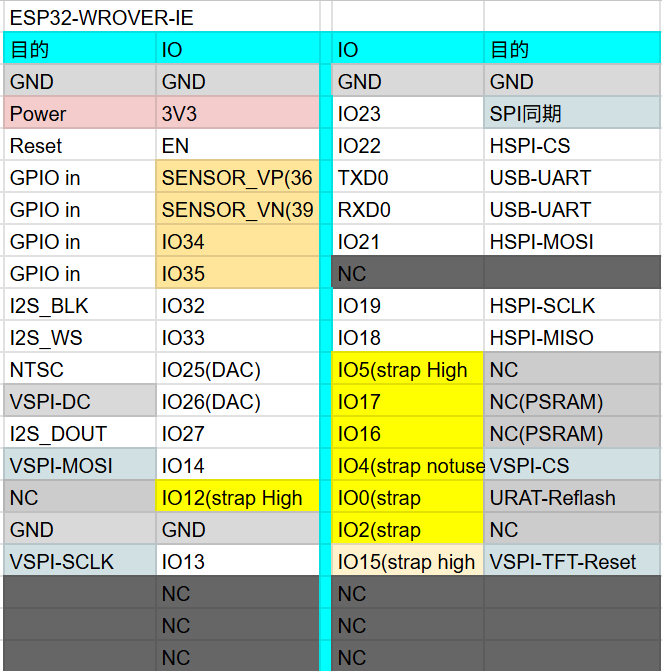
ESP32-WROVER Pin Assignment
I2C
| Bus | SDA | SCL | Notes |
|---|---|---|---|
| I2C1 | GPIO 14 | GPIO 21 | Shared with RTC (RX8900) |
| I2C2 | GPIO 47 | GPIO 48 | General purpose |
Use with I2C.new(unit: "ESP32_I2C0", ...) etc. (see Peripherals > I2C).
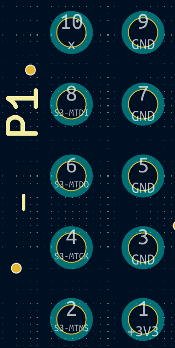
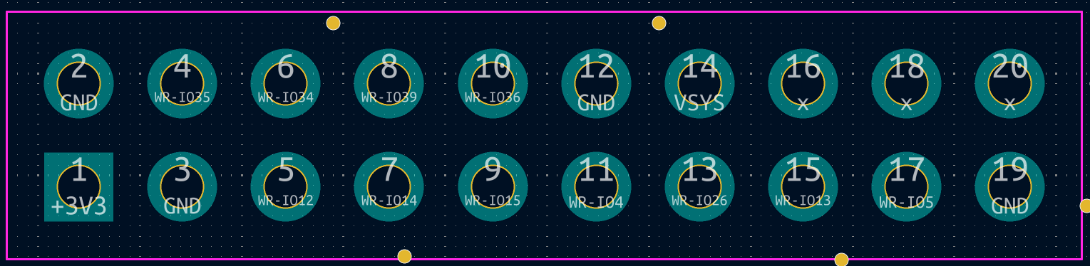
External GPIO
Pin Locations (S3)
Pin Locations (WROVER)
RTC (Real-Time Clock)
The board includes an RX8900 RTC IC (I2C address 0x32, via I2C1). Time is maintained by a battery.
i2c = I2C.new(unit: "ESP32_I2C0")
rtc = RX8900.new(i2c)
rtc.sync_system_clock
See RX8900 API for details.
Related
- Check before using pins: FmrbHw
- Peripheral API: Peripherals
- From boot to your first app: Setup and Connection